- 您现在的位置:买卖IC网 > Sheet目录324 > EK-V6-ML631-G-J (Xilinx Inc)VIRTEX-6 HXT FPGA ML631 EVAL KIT
Virtex-6 FPGA Data Sheet: DC and Switching Characteristics
The GTH transceiver supplies must be powered using a MGTHAVCC, MGTHAVCCRX, MGTHAVCCPLL, and MGTHAVTT
sequence. There are no sequencing requirement for these supplies with respect to the other FPGA supply voltages. For
more detail see Table 27 : GTH Transceiver Power Supply Sequencing . There are no sequencing requirements for the GTX
transceivers power supplies.
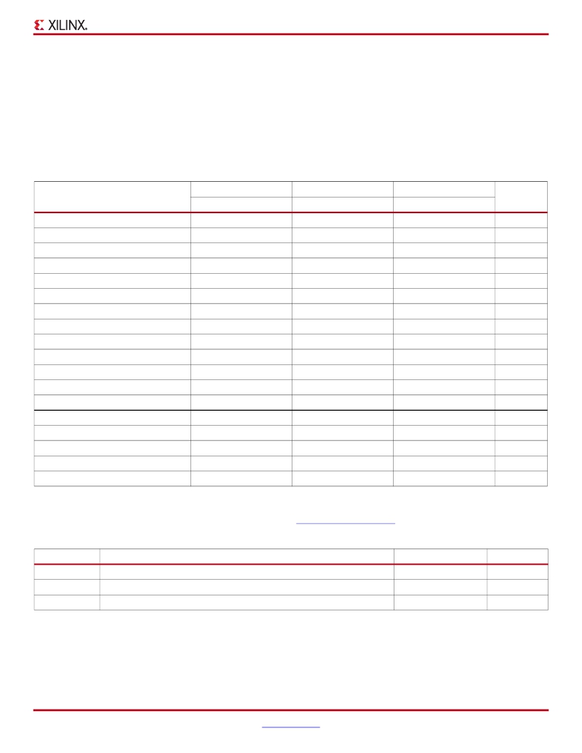
Table 5 shows the minimum current, in addition to I CCQ , that are required by Virtex-6 devices for proper power-on and
configuration. If the current minimums shown in Table 4 and Table 5 are met, the device powers on after all three supplies
have passed through their power-on reset threshold voltages. The FPGA must be configured after applying V CCINT , V CCAUX ,
and V CCO for the appropriate configuration banks. Once initialized and configured, use the XPE tools to estimate current
drain on these supplies.
Table 5: Power-On Current for Virtex-6 Devices
XC6VLX75T
XC6VLX130T
XC6VLX195T
XC6VLX240T
XC6VLX365T
XC6VLX550T
XC6VLX760
XC6VSX315T
XC6VSX475T
XC6VHX250T
XC6VHX255T
XC6VHX380T
XC6VHX565T
XQ6VLX130T
XQ6VLX240T
XQ6VLX550T
XQ6VSX315T
XQ6VSX475T
Device
I CCINTMIN
Typ (1)
I CCAUXMIN
Typ (1)
I CCAUXQ + 10
I CCAUXQ + 10
I CCAUXQ + 40
I CCAUXQ + 40
I CCAUXQ + 40
I CCAUXQ + 40
I CCAUXQ + 40
I CCAUXQ + 40
I CCAUXQ + 50
I CCAUXQ + 40
I CCAUXQ + 40
I CCAUXQ + 40
I CCAUXQ + 40
I CCAUXQ + 100
I CCAUXQ + 100
I CCAUXQ + 100
I CCAUXQ + 100
I CCAUXQ + 100
I CCOMIN
Typ (1)
I CCOQ + 30 mA per bank
I CCOQ + 30 mA per bank
I CCOQ + 30 mA per bank
I CCOQ + 30 mA per bank
I CCOQ + 30 mA per bank
I CCOQ + 30 mA per bank
I CCOQ + 30 mA per bank
I CCOQ + 30 mA per bank
I CCOQ + 30 mA per bank
I CCOQ + 30 mA per bank
I CCOQ + 30 mA per bank
I CCOQ + 30 mA per bank
I CCOQ + 30 mA per bank
I CCOQ + 30 mA per bank
I CCOQ + 30 mA per bank
I CCOQ + 30 mA per bank
I CCOQ + 40 mA per bank
I CCOQ + 40 mA per bank
Units
mA
mA
mA
mA
mA
mA
mA
mA
mA
mA
mA
mA
mA
mA
mA
mA
mA
mA
Notes:
1.
2.
Typical values are specified at nominal voltage, 25°C.
Use the Xilinx Power Estimator (XPE) spreadsheet tool (download at http://www.xilinx.com/power ) to calculate maximum power-on currents.
Table 6: Power Supply Ramp Time
Symbol
V CCINT
V CCO
V CCAUX
Description
Internal supply voltage relative to GND
Output drivers supply voltage relative to GND
Auxiliary supply voltage relative to GND
Ramp Time
0.20 to 50.0
0.20 to 50.0
0.20 to 50.0
Units
ms
ms
ms
DS152 (v3.6) March 18, 2014
Product Specification
7
发布紧急采购,3分钟左右您将得到回复。
相关PDF资料
EK-V7-VC707-CES-G
VIRTEX-7 VC707 EVAL KIT
EK-Z7-ZC702-CES-G
ZYNQ-7000 EPP ZC702 EVAL KIT
EL1848IYZ-T7
IC LED DRIVR WHITE BCKLGT 8-MSOP
EL7156CSZ
IC DRIVER PIN 40MHZ 3STATE 8SOIC
EL7158ISZ
IC DVR PIN 40MHZ 3STATE 8-SOIC
EL7222CSZ
IC DVR HS DUAL MOSFET 8-SOIC
EL7242CSZ
IC DVR HS DUAL MOSFET 8-SOIC
EL7243CMZ-T13
IC CCD DRIVER DUAL HS 20-SOIC
相关代理商/技术参数
EK-V7-VC707-CES-G
功能描述:VIRTEX-7 VC707 EVAL KIT RoHS:是 类别:编程器,开发系统 >> 通用嵌入式开发板和套件(MCU、DSP、FPGA、CPLD等) 系列:Virtex®-7 标准包装:1 系列:PICDEM™ 类型:MCU 适用于相关产品:PIC10F206,PIC16F690,PIC16F819 所含物品:板,线缆,元件,CD,PICkit 编程器 产品目录页面:659 (CN2011-ZH PDF)
EK-V7-VC707-CES-G-J
功能描述:VIRTEX-7 VC707 EVAL KIT JAPAN RoHS:是 类别:编程器,开发系统 >> 通用嵌入式开发板和套件(MCU、DSP、FPGA、CPLD等) 系列:Virtex®-7 标准包装:1 系列:PICDEM™ 类型:MCU 适用于相关产品:PIC10F206,PIC16F690,PIC16F819 所含物品:板,线缆,元件,CD,PICkit 编程器 产品目录页面:659 (CN2011-ZH PDF)
EK-V7-VC707-G
制造商:Xilinx 功能描述:VIRTEX-7 FPGA VC707 EVALUATION KIT - Boxed Product (Development Kits) 制造商:Xilinx 功能描述:KIT EVAL VIRTEX7 VC707 制造商:Xilinx 功能描述:VIRTEX-7 VC707 FPGA EVAL KIT
EK-V7-VC707-G-J
制造商:Xilinx 功能描述:KIT EVAL VIRTEX7 VC707 JAPAN
EKWF111
功能描述:WiFi/802.11开发工具 WF111 SDIO Eval kit
RoHS:否 制造商:Roving Networks 产品:Evaluation Boards 工具用于评估:RN-171 支持协议:802.11 b/g 频率:2.4 GHz 接口类型:UART 工作电源电压:2 V to 16 V
EKWT11-A
功能描述:蓝牙/802.15.1 开发工具 EKWT11-A
RoHS:否 制造商:Panasonic Electronic Components 产品:Bluetooth Evaluation Kit 工具用于评估:PAN1721 频率:2.4 GHz 接口类型:I2C 工作电源电压:2 V to 3.6 V
EKWT11-E
功能描述:蓝牙/802.15.1 开发工具 EKWT11-E
RoHS:否 制造商:Panasonic Electronic Components 产品:Bluetooth Evaluation Kit 工具用于评估:PAN1721 频率:2.4 GHz 接口类型:I2C 工作电源电压:2 V to 3.6 V
EKWT11i-A
功能描述:蓝牙/802.15.1 开发工具 WT11i A Eval Kit
RoHS:否 制造商:Panasonic Electronic Components 产品:Bluetooth Evaluation Kit 工具用于评估:PAN1721 频率:2.4 GHz 接口类型:I2C 工作电源电压:2 V to 3.6 V
